Using Embedded Passives to Transform RF Attenuator & Filter Design
The RF industry faces a critical challenge: traditional waveguide modules and coaxial connector solutions no longer meet the demanding requirements for miniaturization and efficiency in modern RF systems. While printed circuit board (PCB) manufacturing offers promising solutions through cost-effective, high-volume production, conventional surface mount technology (SMT) components present significant limitations for RF applications.
The PCB Challenge in RF Design
Traditional PCB designs rely heavily on surface-mount passive components, which introduce several critical challenges:
- Parasitic effects and matching difficulties between components
- Complex routing requirements that increase losses
- Limited placement options on board surfaces
- Via-related coupling issues
- Potential reliability concerns
Recent advancements in PCB laminate technologies have made these boards increasingly attractive for high-frequency RF applications. They potentially offer advantages over technologies like low-temperature cofired ceramic (LTCC) and high-temperature cofired ceramic (HTCC). However, realizing these benefits requires overcoming the limitations of traditional surface-mount passives.
Embedded Passive Technology: A Transformative Approach
Embedded passive technology offers an elegant solution by directly integrating resistors, capacitors, and lumped element circuits into the PCB structure. This integration happens through thin-film resistor foils and dielectrics incorporated within internal board layers, fundamentally changing how RF circuits can be designed.
Key advantages of this approach include:
- Reduced routing complexity
- Minimal need for vias
- Enhanced circuit reliability and performance
- Optimal utilization of internal PCB layers
- Freedom to use board surfaces for critical components and test points
Technical Implementation
The embedded passive process integrates thin-film resistor foils and dielectrics with copper foil layers, which are then incorporated into PCB inner layer cores. Designers can create sophisticated 2D embedded passive structures through precise patterning and etching.
A unique economic advantage emerges. Unlike SMT components, where costs increase with complexity, the cost-per-component for embedded passives decreases as more components are integrated within a layer. This creates opportunities for both performance improvements and cost optimization.
Advanced Applications
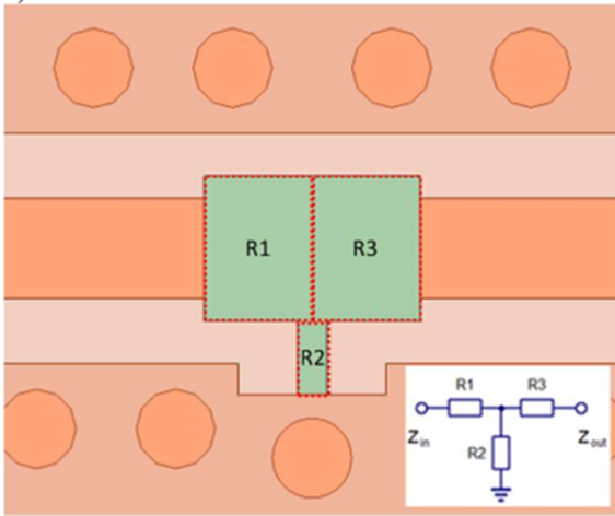
The technology enables innovative approaches to circuit design, such as creating multi-element circuits through strategic shaping of 2D foil and copper layers. For example, T-shaped etched attenuators can be formed from a single resistive foil region with three copper connections. Similar principles apply to filter elements and complete filter designs using resistive and capacitive foil layer combinations.
Looking Forward
As RF systems continue to evolve, embedded passive technology represents a significant step forward in addressing the industry’s challenges of miniaturization, efficiency, and performance. This approach solves current design limitations and opens new possibilities for innovation in RF circuit design.
This blog discussed some of the potential benefits of embedded resistors and capacitive foils in RF circuit applications.
Consult Quantic Ohmega Ticer for more details on how embedded passives can revolutionize your next RF circuit project

Subscribe to the Quantic Electronics newsletter
© 2025 Quantic Ohmega Ticer
© 2023 Quantic Ohmega Ticer


